

Careers
Our work spans semiconductor design, chiplet integration, camera devices and measurement instruments. We are looking for people who want to build hardware with us in a fully integrated, in-house development environment.
Pulse Waveform Analyzer (MCA)
A measurement unit that captures faint analog pulses from a detector as digital waveforms, determines their pulse heights and generates an energy spectrum.
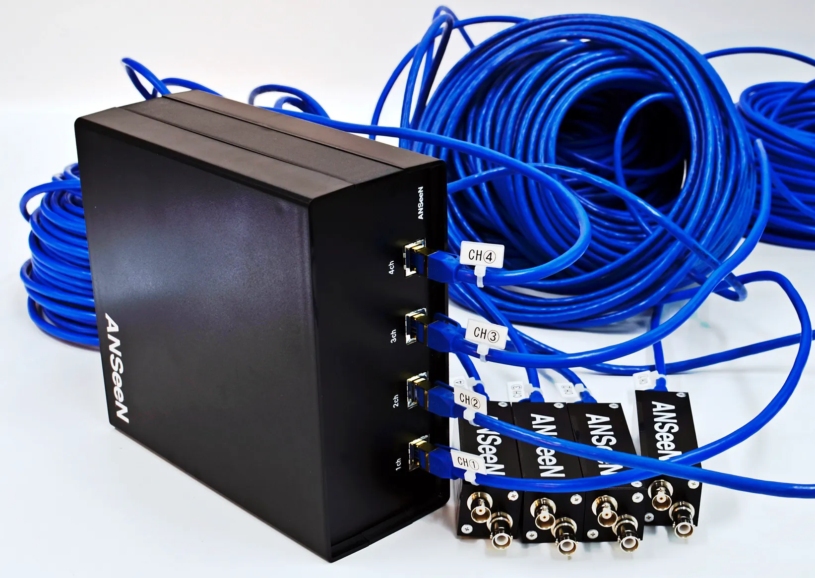
Detection & Signal Processing Layer
Low-noise analog design that amplifies and shapes tiny pulse signals. How well this stage is engineered determines energy resolution.
SKILLAnalog circuit design / SPICE simulation / low-noise PCB layout / hands-on evaluation with oscilloscopes and radiation sources
Digital Processing & Recording Layer (SoM)
FPGA logic and embedded software that process the pulse waveforms output by the ADC in real time, determine pulse heights and build histograms. The SD card stores the configuration in place of an EPROM.
SKILLVerilog / VHDL, Vivado / embedded C, embedded Linux / digital waveform processing (filter design) / high-speed interfaces (LVDS, DDR)
Application & Analysis Software Layer
PC software for setting measurement conditions and collecting data, plus analysis algorithms covering peak identification, nuclide identification and calibration.
SKILLPython / C#, C++ / signal processing, statistical analysis / fitting algorithms / UI design
Power Supply & High-Voltage (HV) Layer
Design of power systems and protection circuits that deliver stable high voltage for detector bias without becoming a noise source for the analog stage.
SKILLPower circuit design / high-voltage insulation and safety design / EMC and noise mitigation / thermal design
CdTe Photoncounting FPD
A photon counting X-ray image sensor built on CdTe and our proprietary ASIC. A large-area detector for medical and industrial non-destructive testing, it builds on the MCA foundation with the technology to make the sensor itself in-house.
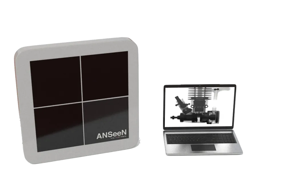
CdTe Crystal & Sensor Process Layer
Electrode formation, surface treatment and dicing of the compound semiconductor CdTe. Performance depends on suppressing leakage current and polarization to achieve stable long-term operation.
SKILLSemiconductor processing (deposition, photolithography, etching) / crystal and device evaluation (I-V characteristics, spectroscopic measurement) / cleanroom practice
Readout ASIC & Bump Bonding Layer
ASIC design of readout circuits that count X-ray photons one by one, and bump bonding that connects the sensor and ASIC one-to-one at pixel pitch.
SKILLMixed-signal ASIC design / circuit layout / flip-chip and bump bonding / bond reliability evaluation
Tiling & Large-Area Layer
Seamlessly arranging small sensor tiles to build a large detection area. This requires µm-order positioning and mechanical designs that stay accurate under heat and stress.
SKILLPrecision mechanical design / positioning and assembly jig design / 3D CAD / tolerance design, thermal deformation analysis
Image Processing & Correction Software Layer
Processing that corrects pixel-to-pixel variation and defects to produce uniform images, and material identification algorithms that exploit energy discrimination.
SKILLImage processing / Python, C++ / statistical processing, calibration design / high-speed processing of large datasets
Common Platform Layer (shared with MCA)
The readout and recording platform is shared with the MCA. It also handles high-speed transfer of image data streams and stable HV supply for sensor bias.
3D-CMOS FPD
A next-generation image sensor with the pixel structure and readout circuitry stacked in three dimensions. It is our newest development theme, with the first prototype currently under evaluation. We are at the stage of exploring uncharted territory: building it from the process up and verifying it through our own measurements.
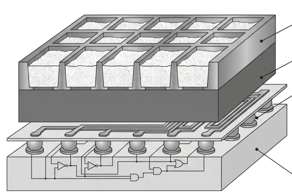
Pixel Structure & Microfabrication Layer
Forming microstructures that partition the X-ray-to-light conversion layer pixel by pixel. Suppressing leakage into neighboring pixels translates directly into resolution.
SKILLMicrofabrication (etching, filling, polishing) / materials processing / structural evaluation by SEM and cross-section observation
3D Stacking & Readout Circuit Layer
Stacking readout circuitry directly beneath the pixels for higher speed and lower noise. The precision and yield of bonds across layers directly determine the product's success.
SKILLCMOS / mixed-signal circuit design / wafer bonding, TSV / process integration
Assembly & Yield Analysis Layer
Mounting prototype chips on evaluation boards and inspecting bonds by SEM, X-ray and cross-sectioning. Identifying failure modes and feeding them back to the process side—this back-and-forth is the substance of development.
SKILLAssembly technology / failure analysis (SEM, X-ray inspection, cross-section observation) / statistical yield analysis / production engineering
Image Acquisition & Image Quality Evaluation Software Layer
Software that captures high-frame-rate images without dropping frames, and a framework that quantitatively compares resolution, noise and sensitivity to judge each prototype.
SKILLImage processing / Python, C++ / high-speed data processing / understanding of image quality metrics (MTF, DQE)
Common Platform Layer (shared with MCA and FPD)
The evaluation board's readout and recording platform is shared across all three products. We build it from the prototype stage with a configuration designed for mass production.
A Development Cycle Shared by All Three Products
From design to mass production, we run everything in-house.
Design
Parallel design of schematics, PCBs, FPGA RTL and 3D enclosures
Prototyping
Parts procurement, assembly, integration and firmware bring-up
Evaluation
Measurements with X-rays and radiation sources; verification of resolution, noise and temperature characteristics
Integration
Combining HW, FW and analysis SW, and calibrating the entire system
Production Engineering
Design of inspection jigs and calibration processes, yield improvement
Mass Production
Shipping inspection, calibration and traceability management
The People Behind Every Stage
These correspond to the layers in each product card. We are looking for people who have deep expertise in at least one area and can speak a common language with engineers in neighboring areas.
Analog Circuit Design
Design of amplifier and ADC circuits that pick up faint radiation signals
Semiconductor Process & ASIC Design
Compound semiconductor (CdTe) and 3D-stacked CMOS processes, mixed-signal ASIC development
FPGA & Embedded Software
FPGA/DRAM control on SoM, embedded Linux, data recording and processing
Application & Analysis Software
Development of pulse-height spectrum analysis, GUI/control software and data processing algorithms
Power Supply & High-Voltage Circuit Design
Design of low-noise power supplies and HV (high-voltage) modules
System Integration & Mechanical Design
Motherboard integration, enclosure design, mass production and reliability testing
Who we're looking for:People who want to see the whole picture, from understanding the underlying principles through mass production and quality assurance. As a small team, the person who designs something also sees it through evaluation and production ramp-up.
Open Positions
We currently accept casual interviews year-round. For details, please contact us via the form below.
Casual Interviews & Technical Consultations
We are looking for people with expertise in at least one area who want to be involved end to end, all the way through mass production. Feel free to get in touch.