

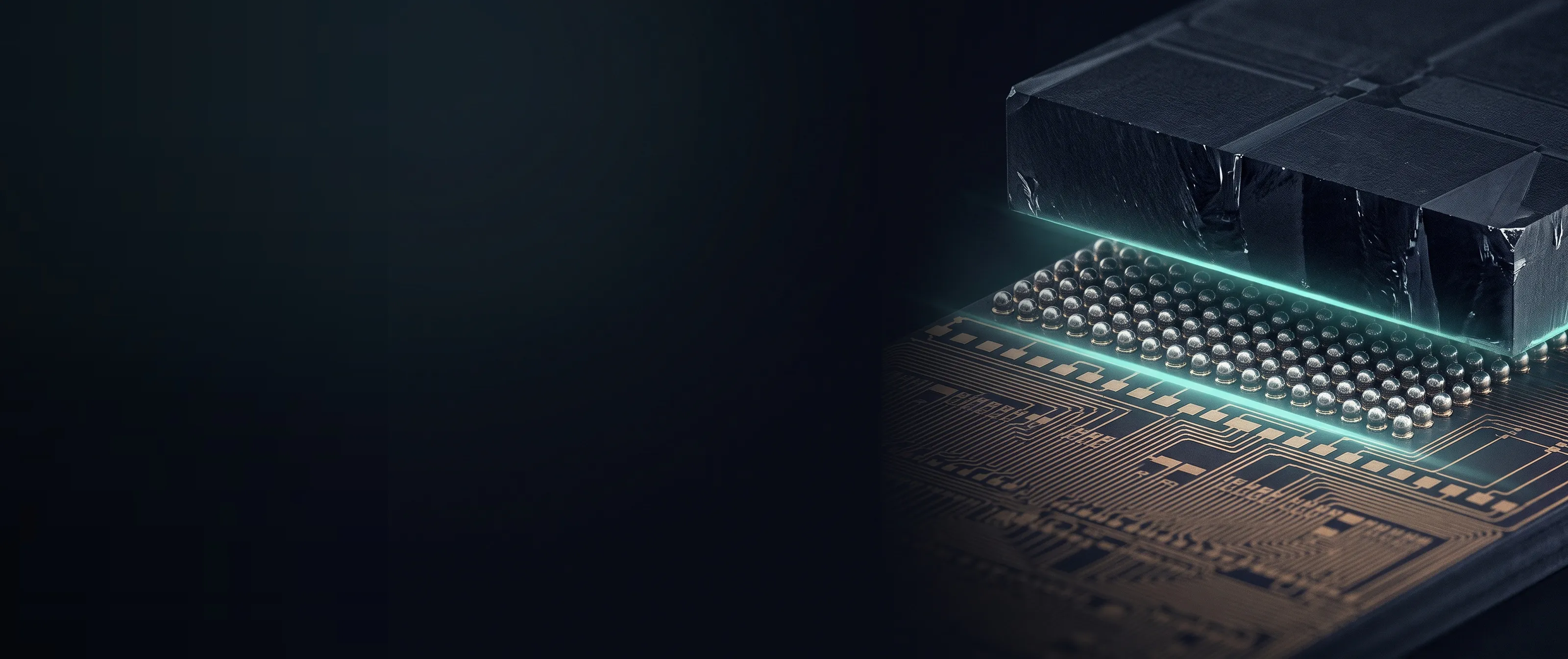
ChipletContract Development
Design, assembly and manufacturing of chiplets (heterogeneous bonding), including compound semiconductors. Not limited to sensors, we take on full custom development to customer specifications.
ChipletContract Development
Design, assembly and manufacturing of chiplets (heterogeneous bonding), including compound semiconductors. Not limited to sensors, we take on full custom development to customer specifications.
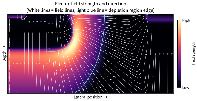
PD Device Design & Prototyping
- MaterialsSi / CdTe / TlBr, etc.
- ScopeDesign and prototyping of detector elements (PD devices)
- StatusBy individual consultation
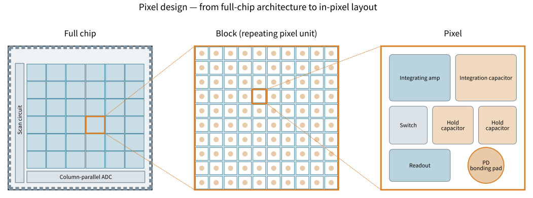
ASIC Design & Prototyping
- StructureHybrid structure (TSV-based)
- ScopeDesign and prototyping of readout integrated circuits (ASICs)
- StatusBy individual consultation
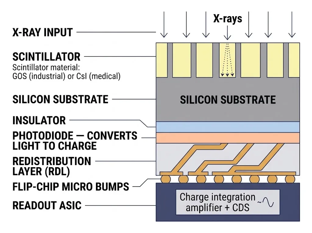
CoW Assembly / Multi-Layer Stacking
- Assembly methodChip on Wafer (CoW) / multi-layer stacking
- BondLow-temperature, low-pressure bonding with bumps of 20μmΦ or less
- StatusBy individual consultation
Development Flow
ANSeeN handles design and overall integration, outsourcing wafer fabrication, 3D processing, stacking and tiling to multiple manufacturing partners (common to CdTe and 3D-CMOS). From consultation to mass production, we proceed while reviewing deliverables at each phase.
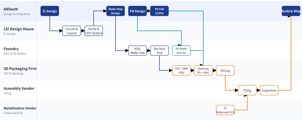
- ProcessConsultation → Specification → Design → Prototyping → Evaluation → Mass production
- Design & developmentDesign of PD devices and ASICs, including heterogeneous bonding of compound semiconductors with CMOS
- Assembly & manufacturingAssembly and supply from prototyping through mass production
Bonding & Assembly Process
Heterogeneous bonding makes two different types of semiconductor, a detector element and an ASIC, function as a single sensor. Our own Imaging products (CdTe PhotonCounting FPD and 3D CMOS FPD) serve as direct proof of this technology.
Consult on Contract Chiplet Development
Consult with us individually on the design, assembly and manufacturing of heterogeneous bonding involving compound semiconductors.
ANSeeN Inc. / TEL: 053-522-7708 / Contact: https://anseen.com/contact/