

CdTe PhotonCounting FPDEngineering sample
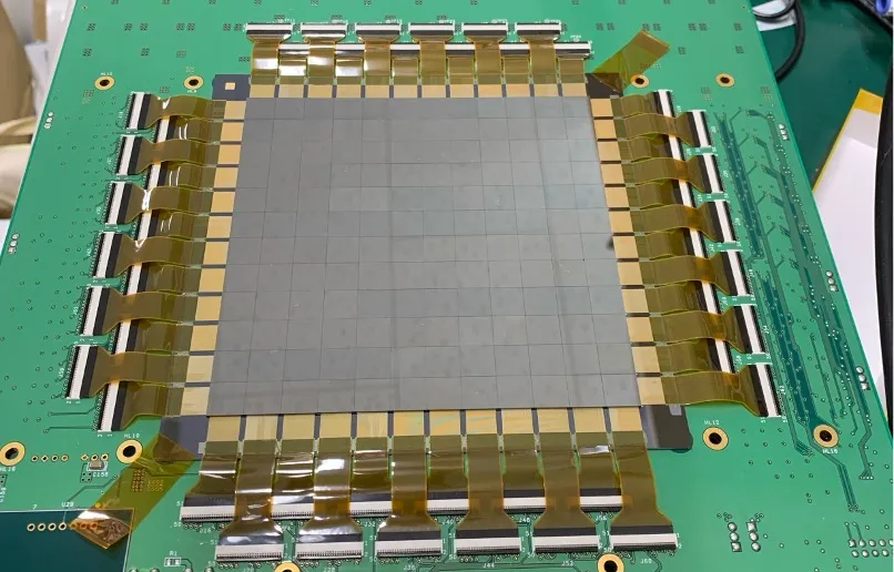
A direct-conversion CdTe photon counting sensor that counts individual X-ray photons and forms images while preserving energy information. With no blur from scattered light, it renders fine structures sharply in applications ranging from non-destructive testing to academic research.
Product photos
Large-area roadmap
Building on the current CdTe PhotonCounting FPD (active imaging area 115.2 x 115.2mm), we will scale up the imaging area in stages using tiling technology.
15 x 15 cm
20 x 20 cm
40 x 40 cm
*Product illustration (3D modeling). Size ratios and module configurations differ from the actual plans. Sizes and timelines reflect current plans and are subject to change.
Specifications
| Name | CdTe PhotonCounting FPD (abbreviated: CdTe FPD) |
|---|---|
| Detection method | Direct-conversion CdTe photon counting sensor |
| Sensor thickness | 750μm / 1000μm |
| Active imaging area | 115.2 x 115.2 mm |
| Pixel count | 1152 x 1152 pixels |
| Pixel pitch | 100μm (2band mode) / 200μm (8band mode) |
| Resolution | 5 lp/mm (2band mode) |
| Maximum frame rate | 60fps |
| Bit depth | 16 bit |
| Energy resolution | 15 levels |
| Number of simultaneously measurable energy bins | 2 bins (100μm pitch) / 8 bins (200μm pitch) |
| Count rate | 2band / 8band each: 5×10⁵ cps; photon counting: 1×10⁶ cps; digital energy integration: equivalent to 1×10⁷ cps |
| Minimum detectable energy | 12.5 keV |
| Operating modes | 2band / 8band / counting / digital energy integration |
| Shutter type | Global shutter |
| Interface | Camera Link (Medium configuration, SDR connector) / convertible to USB3.0 or GbE |
| Power supply | 24V DC / 5A |
| External dimensions | (W)350 x (D)300 x (H)63 mm |
| Weight | Depends on customization |
| Operating temperature | 0 to 30℃ (non-condensing) |
Imaging examples
A selection of actual images and measurement results obtained with this sensor.
Click image to enlarge→ See more imaging examples (gallery)
Technical details
Detection principle and structure
X-rays are converted directly into electric charge inside the CdTe crystal, without first being converted into light. The imaging surface is built by tiling modules in which detector elements and readout circuits are stacked.
Resolution comparison
Because the direct conversion method has no blur from scattered light, even fine lines are resolved separately. We compare it with conventional methods using transmission images of a resolution chart under the same dose conditions and measured MTF values under RQA5 to 8 (tube voltage conditions).
The 3.0 to 5.0 lp/mm region of a resolution chart. Photon counting (left) resolves separate lines up to 5.0 lp/mm, whereas conventional technology (right) merges them into bands.
Measured MTF values. The ANSeeN CdTe FPD outperforms the CMOS system (Full resolution) across all frequency bands.
Flexible sizing through tiling
Because readout circuit signals are routed to the back side through TSVs, modules can be butted together on all four sides with virtually no seams. The imaging area can be enlarged simply by changing the number of identical base modules tiled.
Related patents
Our own patents covering CdTe detector elements, photon counting circuits, and stacking and tiling. For each invention, the registration and publication numbers in each country are listed.
| Technology | Invention | Granted | Published |
|---|---|---|---|
| CdTe detector elements | Method for manufacturing a radiation detection elementManufacturing method for detector elements using CdTe crystals | JP6781868B | — |
| Method for manufacturing a radiation detection element, radiation detection element, and radiation detector including the sameDetector elements using semiconductor crystals such as CdTe and their manufacturing method | JP6758618B | — | |
| Photon counting circuits and pixels | Charge detection circuit and radiation detection device including the sameCharge detection circuit for reading out signals | JP6969734B | — |
| Radiation detector and radiation imaging device including the samePixel layout and sensor structure for acquiring X-ray spectra | JP7201195BKR102807149BTWI806202B | CN114868042EP4071519US2023341571WO2022113170 | |
| Radiation imaging devicePixel drive trigger circuit that reduces circuit power consumption | JP7534739BKR102899421BTWI818339B | CN116390690US2024004092WO2022102095 | |
| Radiation image sensorImplements both photon counting and integration modes in the same circuit | JP7477825BKR102790266B | US2023204799WO2021199195 | |
| Stacking and tiling | Radiation imaging deviceCommunication in a tiling structure that enlarges the area by arranging modules | JP7239125BKR102741153B | US2023008884WO2022074732 |
| Radiation imaging deviceLayout and substrate connection structure that reduce dead space between modules | JP7614592BKR102899416B | US2023378229WO2022074733 | |
| Radiation imaging deviceArrangement of detector element blocks, and stacking and connection via bump electrodes | JP7534743BTWI826931B | CN117042694EP4289360KR20230136198US2024145521WO2022190321 |
*Extracted from our patent data as of May 2026. "Registered" refers to registration gazette (B) numbers; "published" refers to publication gazette numbers. Examination status in each country may change.
Related Articles
ANSeeN Inc. / TEL: 053-522-7708 / Contact: https://anseen.com/contact/