


X-ray Image Sensors
We develop everything in-house, from semiconductor design through chiplet integration to finished camera devices. Building on our current CdTe PhotonCounting FPD, we plan to expand into larger formats using tiling technology.
X-ray Image Sensors
We develop everything in-house, from semiconductor design through chiplet integration to finished camera devices. Building on our current CdTe PhotonCounting FPD, we plan to expand into larger formats using tiling technology.
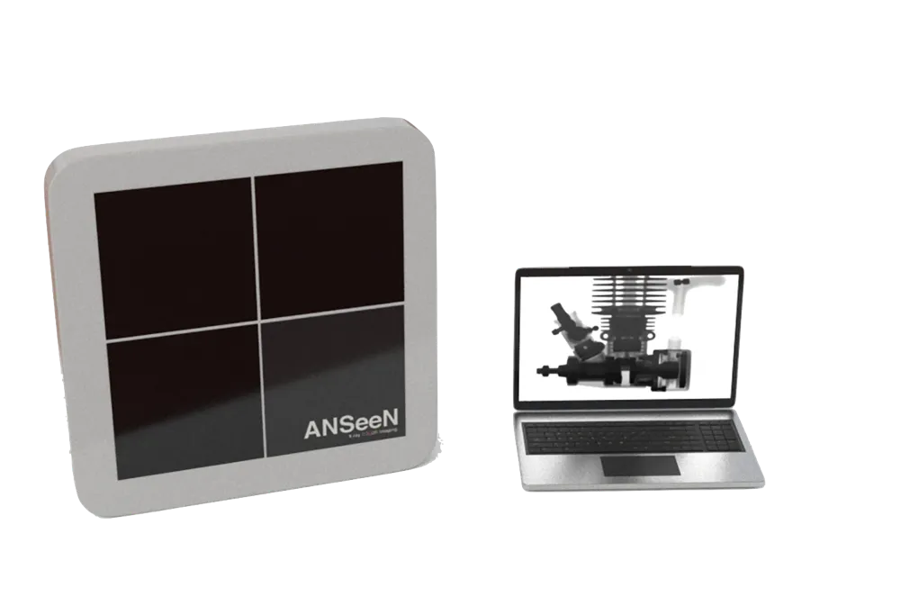
CdTe PhotonCounting FPD
- SensorCdTe
- Detection methodDirect conversion / photon counting
- Active imaging area115.2 x 115.2mm
- StatusEngineering sample
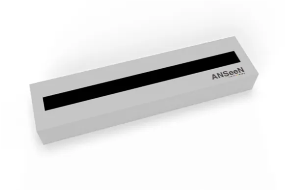
CdTe PhotonCounting Line Sensor
- SensorCdTe
- Detection methodDirect conversion / photon counting
- StatusIn development
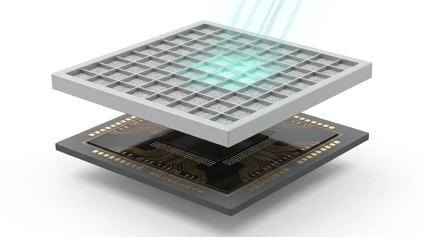
3D CMOS FPD
- SensorPartitioned GoS / Partitioned CsI
- Detection methodIndirect conversion / integrating
- StatusIn development
Contract Measurement and Imaging
We offer contract measurement using the CdTe PhotonCounting FPD and scintillator-based FPDs. For sample evaluations with sensors in development (such as 3D CMOS), see the imaging examples on each product page.
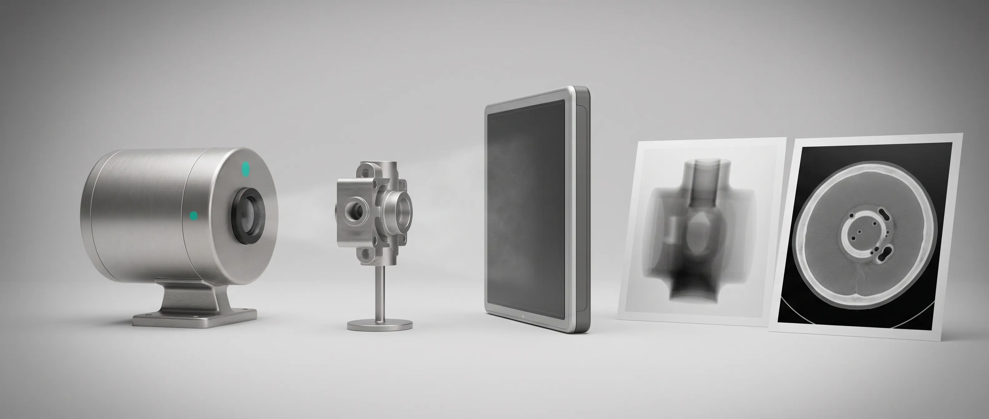
- Supported detection methodsBoth CdTe direct conversion and scintillator-based
- ApplicationsAny imaging need our existing products can cover, including non-destructive testing and material identification
Development and Manufacturing Process
From the semiconductor design at the core of the detector, through chiplet integration, to completion as a camera device. By handling every step of building Imaging products in-house, we can tailor specifications to each application.
Tiling
Because readout circuit signals are routed to the back side through TSVs, modules can be butted together on all four sides and arranged with virtually no seams. Simply changing the number of identical base modules expands the size of the imaging area.
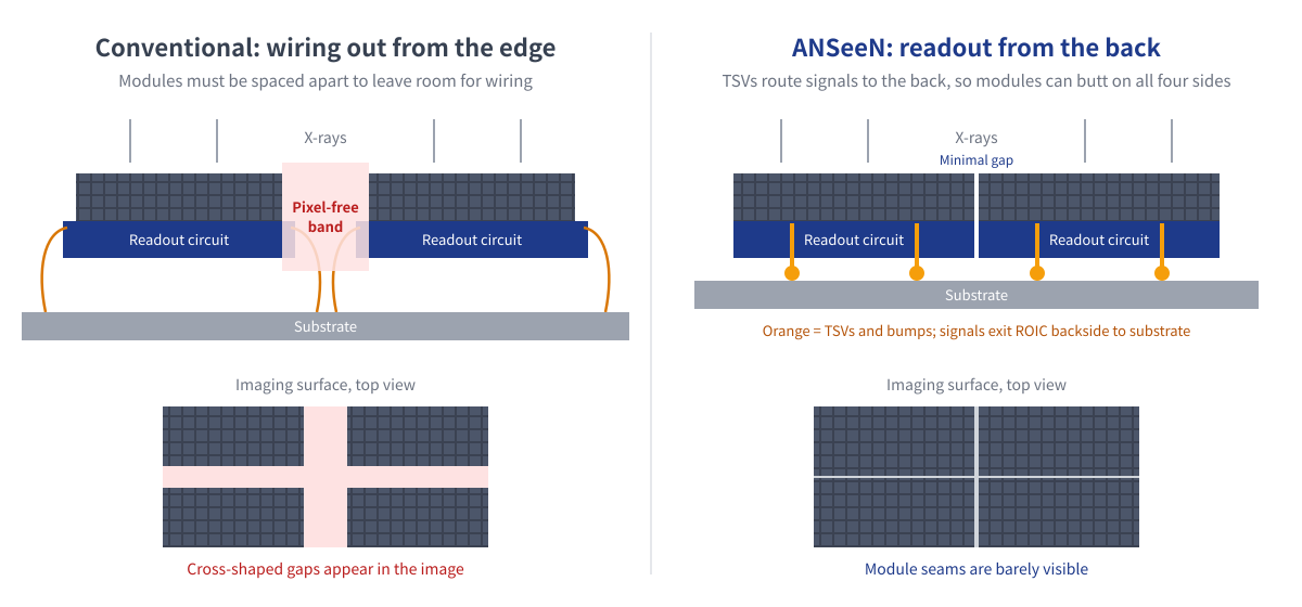
→ See the plan for size expansion through tiling (CdTe PhotonCounting FPD)
Technical Consultation and Sample Evaluation
We handle everything from CdTe PhotonCounting FPD sample evaluations to inquiries about roadmap products and customization.
ANSeeN Inc. / TEL: 053-522-7708 / Contact: https://anseen.com/contact/