

SITE MAP
CHIPLET / PACKAGING

CoW Assembly / Multi-Tier StackingConsultation on request

Stack only known-good chips. Chips selected by die sort are bonded to a target wafer, stacked vertically with TSVs and RDLs, and tiled with small gaps to cover large areas.

PHOTO

Assembled chips

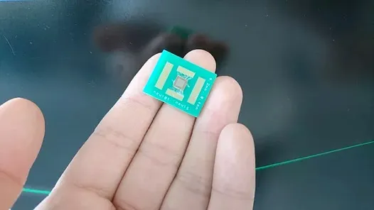
Photo of a chiplet resting on a fingertip
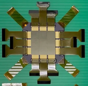
Photo of a die with a detector element bonded to an ASIC
CASES

Case studies

Two processes we actually run for our own Imaging products.

ASIC wafer → TSV + two-layer RDL → μbumps + flip-chip bonding → laser dicing → module testing → tiling on PCB → panel testing

CASE · CdTe

Mounting CdTe on a TSV ASIC wafer, dicing, and tiling

  • Bondingμbumps formed by plating, with CdTe flip-chip bonded (CoW)
  • TestingDiced modules are tested by electrode probing, test pulses and X-rays, and panels are also tested with X-rays
  • Alternative routeRoom-temperature stacking with printed conductive paste → tiling on Si interposers is also supported

The photodiode and readout ASIC are built separately, flip-chip bonded, and tiled into a panel

CASE · 3D-CMOS

Building the PD and ASIC in parallel, bonding, then tiling

  • Separate fabricationThe photodiode and readout ASIC are each built with the process best suited to them
  • BondingKnown-good parts are flip-chip bonded to each other
  • ApproachThe PD and ASIC sides use different foundries and processes. Neither side's constraints carry over to the other until bonding
SPECIFICATIONS

Capabilities

Assembly methodChip on Wafer (CoW) / multi-tier stacking
BondingLow-temperature, low-pressure bonding with bumps of 20μmΦ or less
BumpsPlated μbumps (Sn/Ag) / printed conductive paste (Ag) (allows stacking at room temperature)
Interlayer connectionTSV and RDL (redistribution layer)
TilingArrayed with small gaps on Si interposers / PCBs
StatusConsultation on request
STRUCTURE

CoW and multi-tier stacking

Low-temperature, low-pressure bonding with bumps of 20μmΦ or less preserves the characteristics of delicate compound semiconductors.

  • CoW (Chip on Wafer)Known-good chips selected by die sort are bonded to a target wafer. Defective parts are never stacked together.
  • Multi-tier stackingDetector elements, ASICs and interposers are connected with TSVs and RDLs and stacked vertically.
  • BumpsPlated μbumps (Sn/Ag) and printed conductive paste (Ag). Paste allows stacking at room temperature.
  • TilingStacked chips are arrayed with small gaps on Si interposers or PCBs to cover large areas.

SITE MAP